What Comes After HBM

The memory industry is going through a supercycle for the history books. In 2023 the industry was at the bottom of its worst slump ever, facing negative industry-wide profits. Samsung cut production 50% and both SK Hynix and Micron posted negative gross margins! ChatGPT launched. Stargate alone would require 40% of global DRAM production. HBM became 60% of Nvidia GPU’s manufacturing cost. The three major’s production capacity has been contracted for a year out even though yields on 12-layer stacked HBM3e are as low as 75%. The SK Hynix CEO is still saying the supply shortage will be even worse next year and that demand will outstrip supply beyond 2030. Now all three majors are projected to earn more operating profit in a couple years than Apple does today.
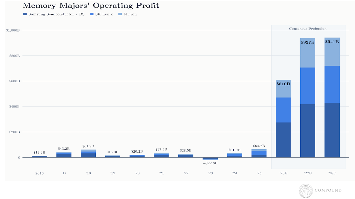
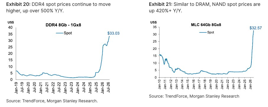
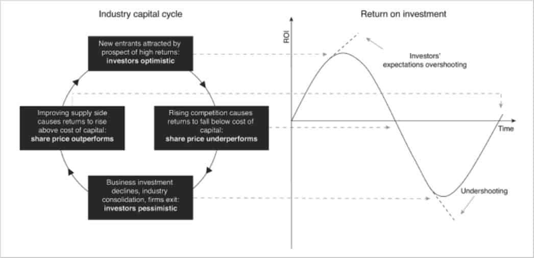
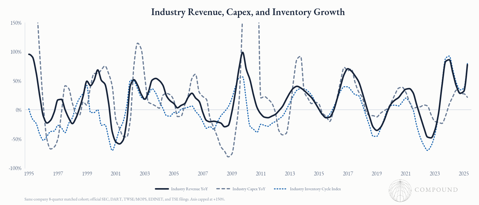
Maybe it’s overly smooth-brained to start a new, technically ambitious company right as we’re nearing the upper end of the capital cycle for an industry so notorious for cyclicality that it’s used as a poster child example in textbooks. But, even if the industry eventually works its way through HBM’s manufacturing challenges, overbuilds capacity, inventory accumulates and the price per stack falls, the underlying demand isn’t going anywhere and memory is no longer a commodity product. Wall Street consensus projects that while prices may ease starting in 2028, the net profit floor for the memory majors will be 5-10x that of the prior cycle. However it pans out, navigating these market dynamics effectively will take a founder well-versed in history and the charts below.
Over the years, we’ve spent a lot of time looking at novel approaches to AI accelerators, especially those harnessing novel physics that give them a potential order(s) of magnitude advantage. The culmination of our research can be found here. In that, we wrote:
“To have a shot at assailing Nvidia’s moats in software, distribution, its 1-year product release and its 2.5-year performance doubling cadences, a startup must harness physics that grant it a realistic path on paper to ~100x efficiency improvement over today’s H100s. Because, that 100x theoretical or "on paper" advantage may actually be 25x in practice. And, by the ~6-8 years it takes even the top chip startups to get a product to market, Nvidia's already churned through 6-8 product cycle upgrades. That 25x practical advantage is now only ~10x the SotA Nvidia chips at launch.”
We feel similarly about this opportunity. While the memory majors may not be quite as ruthlessly well run as Nvidia, they have everything else going for them and capable product roadmaps ahead.
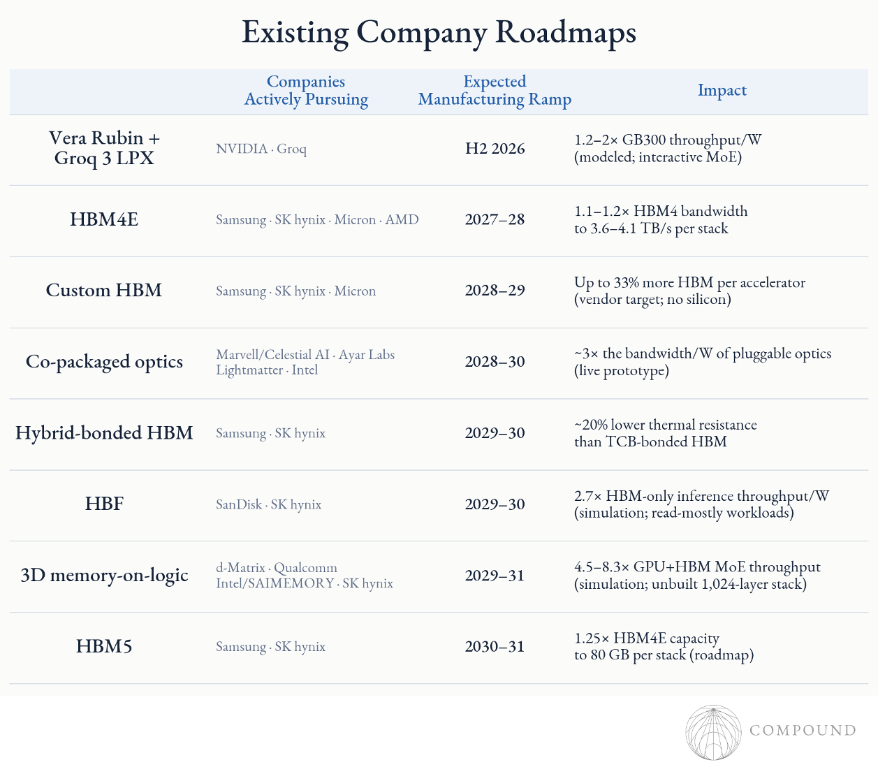
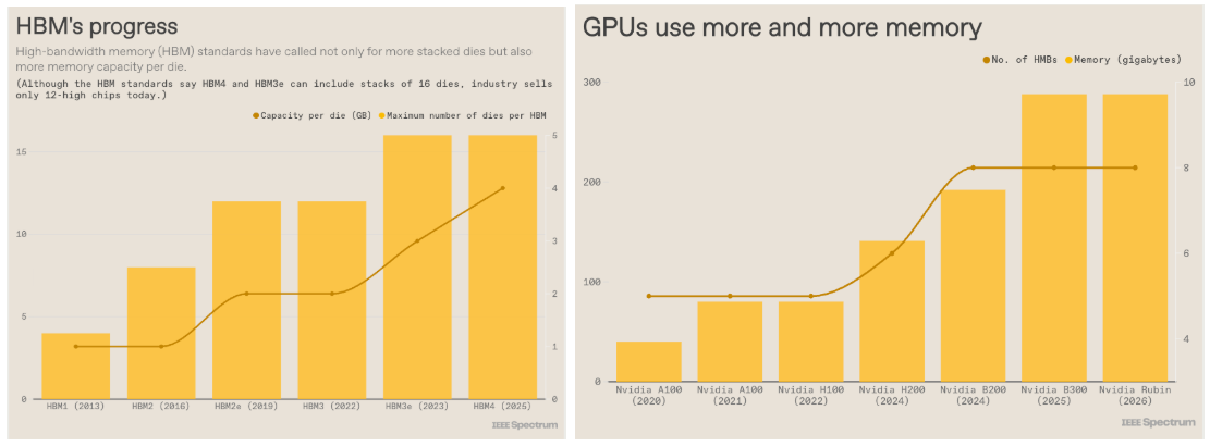
Given that DRAM miniaturization hit a wall over ten years ago and all incumbents are focused on the next-order solutions of ever-more creative advanced packaging means of going vertical, we’d be looking for technologies that side-step these challenges entirely by leveraging entirely different physics that grant them credible paths towards order(s) of magnitude improvement.
For instance, is it possible to absolve the memory wall itself by bridging the bottleneck caused by the speed and energy gap between lightning-fast scratch pad memory SRAM and high bandwidth working memory like DRAM?
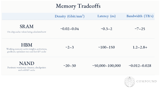
After surveying all the approaches we could find, we think a few could be between one and several breakthroughs away from being viable.
They generally fall into two camps: attempts at HBM-like bandwidth that’s far faster to access or HBM-like bandwidth with NAND-like density.
Faster than HBM Access Speeds
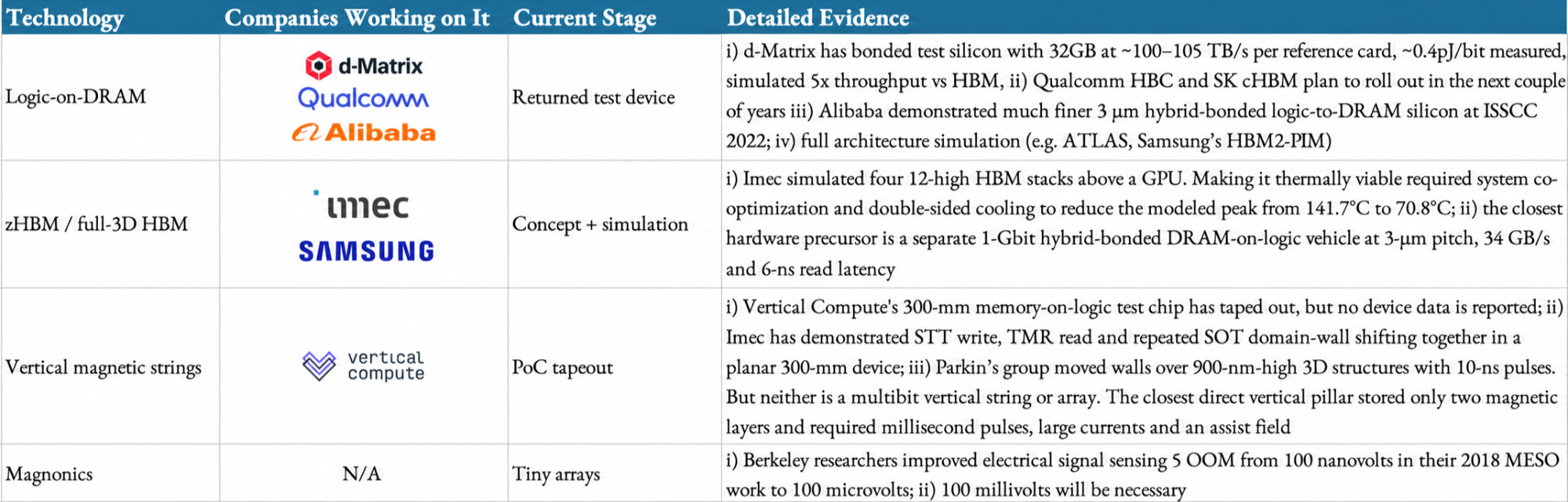
Of the more speculative approaches, the first two that involve pushing DRAM closer to logic are by far the most advanced. d-Matrix and Qualcomm’s approaches could plausibly reach manufacturing within several years. They could have meaningful but not game-changing speed ups. Vertical magnetic strings take this premise of on-die memory farther by using a more radical but risky physics substrate.
We’re particularly excited about magnons, which use spin waves as the information processing unit. Latest research suggests a speculative path towards a non-volatile memory with speeds that approach SRAM access times, DRAM-like density and very low power consumption.
Whereas most magnon research uses metallic ferromagnets, we see antiferromagnetic magnons in insulators as especially attractive because no charge moves through the active material, so dissipation can be very low. And, antiferromagnets’ resonance frequencies can be around one terahertz which puts the relevant dynamics on a 1-2 picosecond timescale vs more than ten times slower for ferromagnetic materials.
The historical problem was readout. Sensing a magnetic state at a scale of approximately 10 nanometers is not trivial, and optical readout does not scale easily. But in the last six years, researchers have increased signal readout over 4 orders of magnitude from ~100 nanovolts to beyond microvolts. They will need to hit 100 millivolts for it to be plausibly commercially useful.
Using these materials, researchers have built a non-destructive read memory PoC.
HBM-like Bandwidth + NAND-Like Density
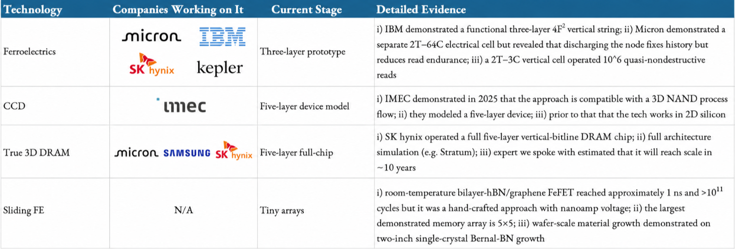
Ferroelectrics has for twenty to thirty years been hypothesized as a potential universal memory platform because it could enable DRAM-like bandwidth, is non-volatile, requires relatively little energy to flip states, and is the most well-understood material system.
Micron even recently invested $1B into demonstrating a device that replaces the DRAM capacitor with a ferroelectric one but otherwise kept the traditional 1T1C charge-sensing set up. The work was shelved because its signal still scaled with capacitor area like DRAM’s so NAND density wasn’t achievable, required sequentially stacking complete 1T1C tiers so had poor cost scaling, and degradation couldn’t be resolved.
Recent academic work has suggested a possible path towards NAND-like density scaling by using 2T-nC vertical strings whereby a given capacitor can be shared across many vertically stacked bits.
While exciting, a startup commercializing such advances in ferroelectrics must contend with the fact that ferroelectrics is closely watched by memory majors. Its technical innovation must yield a decisive advantage, its IP position solid, and it must move rapidly towards manufacturing.
An Accelerated Future
A handful of early-stage memory technologies could yield either far faster access speeds than current HBM or HBM-like bandwidth with NAND-like density.
Beyond distributed near-memory DRAM and true 3D DRAM, technologies like magnonics and vertical FeRAM stand out as being possible platonic ideals for memory.
But they have a very long way to go before being remotely commercially relevant and their estimates below require extrapolating excellent device physics into an array architecture that does not yet exist.
Moreover, even if fundamental hurdles are overcome with the respective materials systems, commercializing the technologies will require founding teams capable of raising $100Ms-1B+. For instance, Micron’s small-scale ferroelectrics demonstration cost $1B. Even developing just a new node within existing memory systems requires 2,000 engineers. That’s not to say it can’t be done, given that companies like Cerebras raised $3B to reach the market with a more complex vertically integrated compute stack.
But if any of these came true, they’d be truly revolutionary transformations of the constraints for AI and how developers think about these systems.
While most of the technologies feel irrelevantly far off and closer to basic science experiments than threats to the memory fiefdoms, we think there’s a possibility their progress could be meaningfully accelerated. We’ve spent years studying materials discovery and translation, including with our portfolio company Orbital Materials.
Our published research details how the advance of NNPs enables high throughput materials simulation at near quantum chemical accuracy, the gap between initial discovery to manufacturing scale-up is slowly being chipped away at. Since then, neural operators for generalized physics modeling, AI engineering tools for CAD and semiconductor-specific design have started to take off. The paths for tech tree exploration could all be run in parallel, orchestrated by agents.
A prime example of this already playing out is OpenAI's recently announced Jalapeño chip, designed largely by AI and appears surprisingly competitive with Nvidia's on OpenAI's first iteration.
Maybe on a 4+ year timeframe these technological tools, combined with the $1T pot at the end of the rainbow, will enable the more exotic approaches to become viable sooner than expected.
Indeed, we saw an analogous thing happen with the novel physics accelerators. thanks to open source libraries like PyTorch and coding agents, companies launched in the last several years have needed far fewer software engineers than the prior generation (Groq, Cerebras, etc) as they haven’t had to write everything from scratch and can move far faster on what custom software they did have to write. We heard something like 50 developers to get to an MVP not 200+.
We’re open to the idea that in the next few years something similar will happen to more basic discovery, translation, and engineering.